A brief tutorial on phase jitter by IDT. Jitter terminology can be confusing and this video attempts to explain phase jitter in a concise format. The correct terminology is RMS phase jitter which is derived by integrating the area under the curve of a specific phase noise plot, at a specific carrier frequency, with a defined frequency range & offset. Presented by Sam Staker, Field Applications Engineer at IDT. Learn more about IDT’s leading timing solutions at http://www.idt.com/go/Clocks.
Hello. Welcome to ‘Time Out’ from IDT; the Number 1 world leader in timing solutions. My name is Sam Staker, and I’m a field applications engineer for IDT. Today we’re going to talk about an important question: What is phase jitter?
Before we do that, let’s talk a little bit about the terminology involved. Jitter can be very confusing. There are a lot of terms, engineers use them in different ways depending upon different applications: Phase jitter, phase noise and others. Before we get into phase jitter and phase noise, let’s take a step back and talk about jitter.
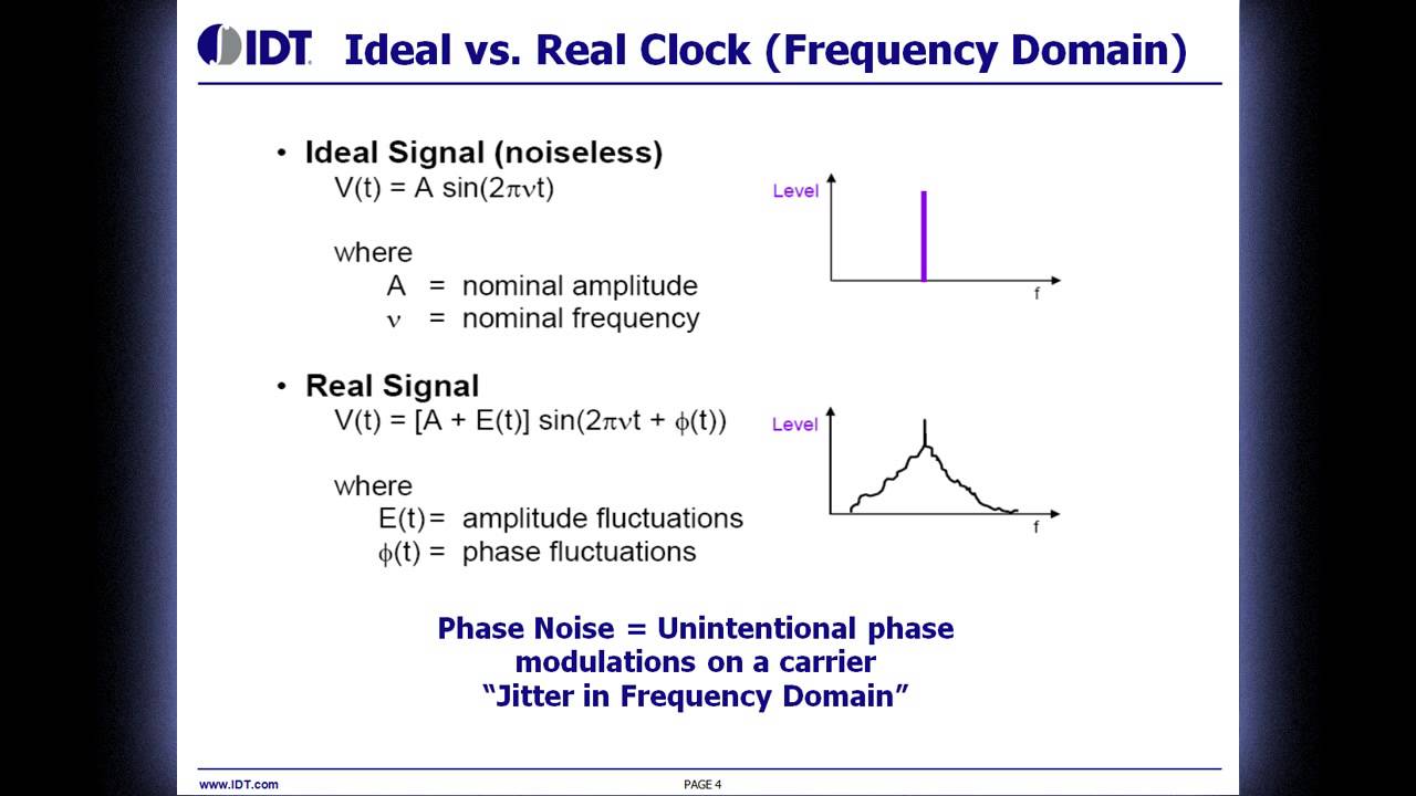
The easiest place to understand jitter and the easiest place to start off is the time domain. We’ll look at an ideal clock signal versus a real-world clock signal. The picture on the top is an ideal clock. The signal period T is constant; the clock frequency, which is the reciprocal of time, is also constant. The rise and fall time is constant, it does not change. Obviously, this waveform is only seen in textbooks. On the bottom is a picture of a real world clock signal; the signal period varies, the frequency changes, the rise and fall time varies. This is the kind of clock signal that engineers see on oscilloscopes in their systems today. Jitter, very simply, is the deviation in time from the ideal reference clock. The picture on the top has no jitter; the picture on the bottom has jitter.
If you remember from engineering and math, if you do a 4EA transform, you can take a signal and move it from the time domain to the frequency domain. If you do a 4EA transform on that top signal, which is the signal without jitter, you’ll get a nice-looking pulse that’s represented here. That pulse is of amplitude A, which corresponds to the amplitude of a clock signal, but instead of a clock signal that goes up and down, you’ll get a pulse that is at the location of that clock frequency. Really what you get in the real world, though, is what’s on the bottom. If you do a 4EA transform on a real-world clock, you’ll get something that looks like the picture on the bottom right. Obviously, most of the energy will be at that main frequency that’s represented by the peak, but instead of dropping off dramatically after that, it’ll drop off to the left and to the right. Those drop-offs, those ramps, are really defined by the error in that signal; the fluctuations in amplitude, the fluctuations in phase. Phase noise is the unintentional phase modulation on that specific carrier frequency. It’s the noise on the clock. The easiest way to think about it, it’s jitter, but its jitter in the frequency domain instead of time domain.
If we look at this frequency domain jitter, we’ll map it out in what we call a phase noise plot, and that is represented here. This is a specific example of a 100MHz carrier frequency or a 100MHz operating frequency, which is the peak that’s centered there in the middle of this graph. On specific applications, engineers may or may not care about this entire graph. In high-speed data coms, which is really a huge growing segment for these devices, they’re only going to look at a very small portion of that graph. That’s represented by that gray box down on the right. That frequency, that box, that range, is offset from that 100MHz carrier. That’s a frequency offset range, a frequency offset mask, or we’ll also call it a jitter mask. We’ll zoom in on that here in the next slide.


Comments